New Semiconductor Devices for IoT Era.
From light-assisted processes for fabrication and integration to applications in opto-electronics
Introduction
In the age of the Internet of Things, sensors have become extensions of human perception — enabling us to detect subtle signals once ignored or inaccessible. Each new sensor technology unlocks new forms of data, allowing us to measure physiological, environmental, or mechanical parameters using miniaturized, low-cost, and non-invasive devices. This paves the way for novel applications in healthcare, safety, environment, sport, and well-being.
Over the past decade, the French and Taiwanese partners of the E-Light project have developed a range of innovative, light-assisted sensor technologies, combining expertise in sol-gel chemistry, nano-optics, and materials engineering.
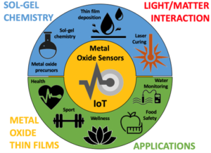
Figure 1. Schematic view of the process that we will develop involving preparation of metal oxide precursors solutions, thin films and curing by laser. Targeted applications are metal oxide sensors prepared at room temperature on various substrates such as glass, plastics, nanocomposites, textiles. Low-cost, versatile integration process makes it possible to develop new applications in the field of Internet of Things (IoT).
Health and Sensor Applications
One major focus has been the development of gas sensors for exhaled breath analysis, enabling non-invasive medical diagnostics. Among them, an ammonia detection sensor has been successfully validated through clinical trials in Taiwan, showing strong potential for early detection of chronic kidney disease in at-risk populations.
At the same time, the teams have developed sensors for motion tracking, relevant to age-related mobility disorders and performance monitoring in competitive sports (e.g., skiing, mountain biking).
A Unique Approach: Light-Driven Fabrication
Rather than relying on traditional high-temperature annealing, E-Light proposes an alternative: using laser irradiation to activate and process sol-gel metal oxide semiconductors. This light-based method allows the fabrication of fully functional devices on a wide range of substrates — including 3D-printed objects and ultrathin, flexible, food-grade packaging films.
This low-energy, substrate-compatible approach opens the door to scalable, sustainable, and application-driven sensor manufacturing.
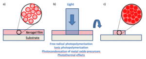
Figure 2. The different options for laser curing of sol-gel thin films.
Scientific Scop of the Project
Long-Term Vision
In the first phase, E-Light focuses on metal oxide-based sensors processed by light-induced techniques. The project will then expand to include related fields such as organic electronics, plasmonics, and advanced nanofabrication, supported by both partners’ research networks.
E-Light is where light meets matter — to create the next generation of intelligent, responsive, and sustainable sensors.
Actions
The priority actions foreseen under this project are
- Student exchanges: Masters, PhD with a priority for co-supervised PhDs. We plan to launch a new co-supervised PhD in September 2024.
- Mutual visits to PIs for brainstorming, preparation of applications for calls for proposals (ANR PRCI, EU projects, etc.) and follow-up of ongoing projects.
- The regular organization of workshops on the main topic and its extension to related topics, which will allow us to build a strong and permanent FR-TW collaboration network around this IRP, based on the complementary networks of the two PIs of this project.